Post-COVID global semiconductor market has grown exponentially with $590 billion in 2021 and also expected to grow to $1 Trillon by 2030. The driving force of this tremendous growth is the technologies such as Artificial Intelligence(AI), Electric Vehicle (EV), 5G,Internet of Things (IoT), Health Care etc. Realization of these technologies, depend on the production of silicon chip for the hardware required. Many chip-making industries in R&D, design, manufacturing, testing, etc. are established to fill the gap in the chip supply chain. Government of India announced semiconductor scheme with an outlay of Rs 76,000 crore in December 2021 to fulfil Aatma Nirbhar Bharath to contribute significantly to the global semiconductor market. Various initiatives are taken in industries, business and academics to ensure robust and sustainable semiconductor ecosystem in India
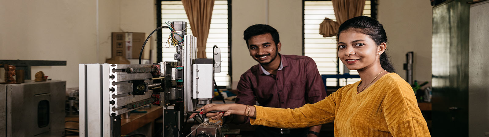
Bachelor of Technology in Electronics Engineering (VLSI Design and Technology) is the specialization of B.Tech in Electronics and Communication Engineering. VLSI is the process of design and manufacturing of Integrated Circuits (IC) or silicon chips. This programme aims to cater to the exponential rise in demand for semiconductor talent pool in India and across the globe. It prepares market-ready engineers in the field of semiconductor technology and electronics industries.
As India focuses on becoming a chip-making nation, the All India Council for Technical Education (AICTE) has also designed a curriculum for B.Tech in Electronics (VLSI Design and Technology). Our course is structured in line with the AICTE model curriculum and covers a range of topics from semiconductor device fundamentals, analog and digital circuits to VLSI circuits and design, IC design and technology, semiconductor equipment operation, manufacturing, assembly, testing and packaging, microcontrollers, embedded systems. It also includes study and usage of Electronic Design Automation (EDA) tools and the programming, scripting languages for semiconductor design, synthesis, simulation, fabrication and testing.
Career prospects :On successful completion of the course, graduates are recruited in Fabless design companies, Display Fabs, Semiconductor Fabs, Fabs for Compound Semiconductors, Silicon Photonics, Sensors, Discrete Semiconductors and Semiconductor Assembly, Testing, Marking, and Packaging (ATMP) / OSAT facilities. The starting salary in a VLSI company varies from Rs 3 lakhs to Rs 20 lakhs per annum, with an average annual salary of Rs 14 lakhs. In core multinational companies the average annual salary for beginners varies from Rs 30 lakh to Rs 80 lakh.
The various schemes and policies are framed by Govt. of India to encourage start-ups, MSMEs, industries and large business houses. Also, Chips to Startup (C2S) programme of Ministry of Electronics and Information Technology, Govt. of India is aiming to train 85,000 Engineers (Bachelors, Masters and PhDs) in ESDM over the period of 5 years.
For any information regarding the admissions,mail us at: info@nitte.edu.in

Ms. Rhea Rodrigues
- DepartmentComputer Science & Engineering
- Designation Pursuing Ph.D in Oncology and Cancer Biology
- Organization University at Buffalo, New York
"NMAMIT allowed me the opportunity to take on new ventures. It could be pitching ideas for workshops or participating in projects that benefit society. Through these opportunities, I gained the confidence to make career-enhancing decisions. In addition, I would like to thank my professors for supporting me throughout my academic career."
Mr. Amol Revankar
- DepartmentComputer Science & Engineering
- Year of Passing 2019
- Designation Software Engineer
- Organization Accenture
"NMAMIT is an amazing place for students to build their skills and aptitude. The teaching staff are excellent in their fields. Students are great learners. The college not only focuses on academics but also on extra curricular activities promoting students' growth. Summing it up, I say, 'It was an honor for me to be a part of NMAMIT".

Ms. Deeksha Bangera
- Department Computer Science & Engineering
- Year of Passing 2019
- DesignationGraduate Engineer Trainee
- Campus RcruitedMercedes Benz
It was a wonderful experience at NMAMIT, Nitte. The faculty members were always encouraging and supportive. The pre-placement activities were very helpful with all the mock tests and training sessions.

Ms. Deeksha S N
- Department Computer Science & Engineering
- Year of Passing 2019
- DesignationSoftware Development Engineer
- Organization Oracle India Private Limited
I am indebted to NMAMIT for providing me excellent lecturers in my M.Tech programme and opportunities to develop my professional personality. NMAMIT has an amazing Placement cell that invites the best of companies to get their students hired for good positions. I express my deep gratitude to all my teachers of NMAMIT. I had the best facilities -a good library, labs, canteen, hostel, indoor and outdoor sports. I shall always remain grateful to NMAMIT.
Mr. Manjunatha U
- Department Computer Science & Engineering
- Year of Passing 2019
- Designation Graduate Engineer Trainee
- Organization Mercedes-Benz Research and Development India
My 4 years in college has been absolutely wonderful at NMAMIT. I have been extremely lucky to have professors who made my academic life comfortable thereby providing me time to explore other interests, opportunities to test my skills in various arenas - from technical clubs to sports clubs, from student chapters to college fests.
NMAMIT continuosly supports students by mentoring and counselling from the time of their entry to exit. They also have strict policies against ragging and sexual harassment to provide a safe eco space for growth of all individuals.
I cannot thank the Placement Department enough for the platform they provided for my career. My experience of college life has turned me into a wholesome person, ready to face new challenges in life every day and I wholeheartedly thank each and every one at NMAMIT who have made my college life memorable.
Ms. Pallavi
- Department Computer Science & Engineering
- Year of Passing 2014
- DesignationSenior Software Engineer
- Organization Happiest Minds Technologies Ltd.
"At NMAMIT, I have received equal opportunities in curricular and extra curricular activities. The institute has an outstanding library with a plethora of books for all disciplines of engineering. The faculty are co-operative and provide vital course materials and throw light on open queries throughout the engineering journey. Various companies visit the campus for placements. The placement department simultaneously provides required training and study materials to prepare every individual for interviews and to pursue their future endeavours."
Ms. Preethika Anchan
- Department Computer Science & Engineering
- Year of Passing 2019
- DesignationSolutions Engineer
- Designation VMware
"My sincere appreciation and gratitude to all the staff of NMAMIT and Abhyuday, the Training & Placement Department for their efforts in imparting quality technical education and aptitude training. I am forever grateful to them for helping me to grab the amazing opportunity that came into my life of being a part of VMware".

Mr. Rameez Shuhaib
- Department Computer Science & Engineering
- Year of Passing 2018
- DesignationSoftware Engineer
- Organization Shuttl
"The NMAM institute of Technology has always provided me an opportunity to broaden my skills and to focus on my areas of specific interests in Academics. The friendly attitude of the professors and their willingness to readily offer a helping hand has helped me to improve technically as well as personally. I'm proud to be an NMAMITian".
Mr. Shashank S Shetty
- Department Computer Science & Engineering
- Year of Passing 2018
- DesignationSoftware Engineer
- Organization MakeMyTrip & Goibibo
"Education is the passport to the future, for tomorrow belongs to those who prepare for it today."- Malcolm X
I am grateful to NMAMIT, Nittefor providing me opportunities for growth. I had an amazing college journey. “To reach the top of the ladder, one should have a great foundation” they say. NMAMIT has given me just that to improve my professional and soft skills. Students in NMAMIT have the benefit of exposure to the challenges of modern technology. They have opportunities to upgrade their skills with a number of events & activities within the college and at inter collegiate levels. NMAMIT has an amazing bunch of experienced faculty. I have benefited greatly from the friendly, supportive student-teacher interactions. Students and teachers strive to reach higher by stretching their limits.
The college has a very approachable Placement department, where anyone can seek help, be it academic, personal or career related. I have benefited a lot from this. The campus placements are growing constantly with top firms visiting NMAMIT and the placement numbers steadily rising. I would strongly recommend my friends and family to consider NMAMIT as their college of preference.
Ms. Siri Vikyath
- Departmentcomputer Science & Engineering
- Year of Passing 2018
- DesignationSenior Quality Assurance Engineer
- Organization Informatica
"My college has played a very important role in the larger journey of my life. It has helped me get where I am today. I will always be grateful to NMAMIT for helping me grow. I am a proud NMAMITIAN. "

Ms. Vandana Nayak
- DepartmentComputer Science Engineering
- Year of Passing 2018
- DesignationSoftware Development Engineer
- Organization IBM India Software Labs
NMAMIT, Nitte has gained immense popularity for the quality of education, faculty and the amazing placement opportunities it offers. The college management is really good and the environment very pleasant and green. Placement department works extra hard to get most of the students placed in reputed companies. Four years of my journey in this college was incredible and lively. Cheers!!

Ms. Varsha P
- DepartmentComputer Science Engineering
- Year of Passing 2018
- Designation Software Engineer
- Organization Informatica
"I joined NMAMIT with hopes of graduating with a job in hand. (I had been allocated a seat in a college in Bangalore but desired to study in my native place and the best choice was NMAMIT.) The advantage of NMAMIT over other colleges in the city is the beauty of nature we get to witness, the humane nature of the people, and the encouraging teachers. They are supportive inside and outside the classroom with academic and extra curricular activities- cultural or sports or just about anything. NMAMIT faculty are like family . They live and teach by example. My journey of 4 years in NMAMIT was joyful and memorable. I have learnt valuable life' lessons along with the curriculum. The brilliant minds at Abhyuday, Placement, make my college truly the best experience one could ever have.
Mr. Vineeth Bangera
- DepartmentComputer Science Engineering
- Year of Passing 2014
- DesignationUX Designer
- Organization NetApp
"I'm fortunate to have found great mentors at NMAMIT who have molded me to explore beyond my horizon by encouraging me to conduct activities that were not limited to a single domain. This ability to think creatively and laterally has definitely helped me find answers during challenging situations. Furthermore, I strongly believe the NMAMIT community including the staff, alumni, and my peers have played a crucial role in my professional career."

Mr. Akshay Kumar
- Department Computer Science
- Year of Passing 2016
- Designation Lead Software Developer
- Organization Collins Aerospace
Well, it is often said “Your attitude, not your aptitude, will determine your altitude”. NMAMIT has been that source which has fine tuned my attitude to help me reach the altitude where I stand today. From enhancing one's self confidence to exploring the credibility, to dream bigger and proceed towards achieving the goals our educational institutions and the faculty, play a major role. I am extremely happy that I got an opportunity to be a student of this wonderful institution which has shaped every individual to come out with flying colors in their life.
The confidence imbibed in each and every student and the support rendered by all the faculty members in NMAMIT is immense and this leads to self development of an individual. Ample opportunities have been provided by the institution to improve oneself in academics as well as extra - curricular activities which definitely enhances the leadership skills in an individual. I am thankful to each and every teacher who has helped me to be a better person in all four years of Engineering. Finally, it is believed that "Education is the passport to the future, for, tomorrow belongs to those who prepare for it today", so keep preparing, keep improving, keep exploring and never give up on your dreams.

Mr Glenn Thomas Alex
- Department Computer Science & Engineering
- Year of Passing 2019
- Designation Proactive Customer Success Engineer
NMAMIT has always been my second home. It's where I discovered a part of myself, and who I wanted to become. Hearing the word 'Nitte' makes me smile and that's the place I want to go back to, if given a chance.This is why I try my best to help the juniors in their academics, especially with regard to placements, because the outstanding feature of this college is the brilliant placements offered at the end of 4 years.

Mr Kartikay Dwivedi
- Department Computer Science
- Year of Passing 2016
- Designation Cloud Infrastructure Administrator
- Campus Recruited VMware
The three most important factors influencing success for an engineer are ' Learning Environment, Branch of interest and opportunity for Placements'. NMAMIT provides all three - the ideal atmosphere for learning, best faculty (as I had in CSE who are also friendly and helpful) and, good placements.
Abhyuday, the counselling, welfare, training & placement department works efficiently with concern, to groom all the students to prepare them for life and find placements in the best possible companies. (Placements begin on entering the final year), I even had the rich privilege and freedom of running a program to train the 3rd year students to prepare for placements along with a team of like minded campus recruited students, a process that trains us in compassionate leadership.
